Well, what can I say about the IDE interface...
At the beginning the ide interface was not much more than a few address and databus
drives used to move the logic that at that time was located on a isa-board onto the
harddrive itself. From this step manufactures hoped (and they were right) that the could
move more "intelligence" into the drive. For example error correction and
mapping of defect sectors were much more easily to implement.
In contrast to scsi interface adapters is an ide interface fairly cheap to implement.
The most basic implementation (and that's what I tried to implement here) does only need a
few "or" gates to implement the host part of the interface.
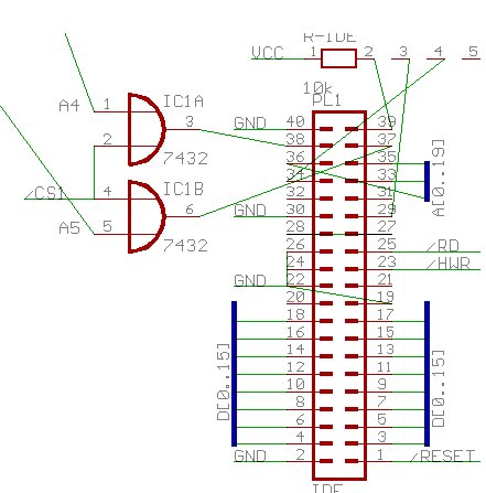
The cable from host to the drive can be devided into this components:
D0-D15: The databus between host and drive. Although 8 bits are allowed, most modern
drives will use the whole 16 bits (to speed up the transmission).
A0-A2: The Addressbus used to address the 16 possible registeres as defined in the ide
standard.
/CS1, /CS3: chipselect lines used to select the (memory mapped) registeres of the
attached drive.
/IOR, /IOW: lines used to indicate read resp. write access to the drive.
/IORDY: may be used by the drive to indicate that it needs more time to complete the
current command. This signal is optional
/RESET: if low, the drive will perform power test on and selftest.
/IRQ: lowered by the drive to indicate that either the last command completed or an
error condition occurred.
The other lines are used to implement dma transfer and to support two drives on the
same cable... These lines are (by the way) the reason why one should not connect more than
one drive to the same ide connector: If two drives are connected to the same connector,
they both share the same register "space", ie., a write to the registerset of
drive A will allways overwrite the contents of drive Bs registers! The ide command set
uses a special bit in the command register to distinguish between drive A and drive B.
Therefore it is impossible for a multitasking OS to address both, drive A and drive B at
the same time neglecting the effect of overlapping access.
You should have wonder: How can only three adresslines access 16 registers? The answer
is simple: /CS1 and /CS3 are used in combination with A0-A2 to select a 8 register
"bank".
/CS1=false, /CS3=false: drive not accessed
/CS1=true, /CS3=true: illegal combination
/CS1=true, /CS3=false: access to the command block registerset (8 regsister)
/CS1=false, /CS3=true: access to the control block registerset (8 register)
Commands are transfered via the command register. First one has to fill the remaining 7
register of the control block before finally the requested command may be written to
the command register. Commands comprise the following classes:
read data - access the datacache or get some status data from the drive. reading is
uncommited, ie., the host must take care that he does not read data faster than the drive
can supply new. The problem is, that the drive has no way to tell the host that the next
data element has been set up.
write data - write data to the drives internal cache or writes state information to the
drive. As when reading data, the drive has no way to tell the host that its ready to
accept the next data element.
control command - eg., lockdrive, selftest, unlock, or identification
vendor specific - semantic not defined by the ide standard.
Those of you, who want to know more about the commandset as well as the physical
connection between host and drive should try to get the ansi working draft for the ide
interface:
[1] [ANSI X3.221 - 199x, ASC X3T9.2 Working Draft, Revision 4,
17-MAR-1993]
|